- 您现在的位置:买卖IC网 > Sheet目录366 > TMDXEVM5515 (Texas Instruments)EVAL MODULE DSP FOR C55XX
SPRS645F – AUGUST 2010 – REVISED OCTOBER 2013
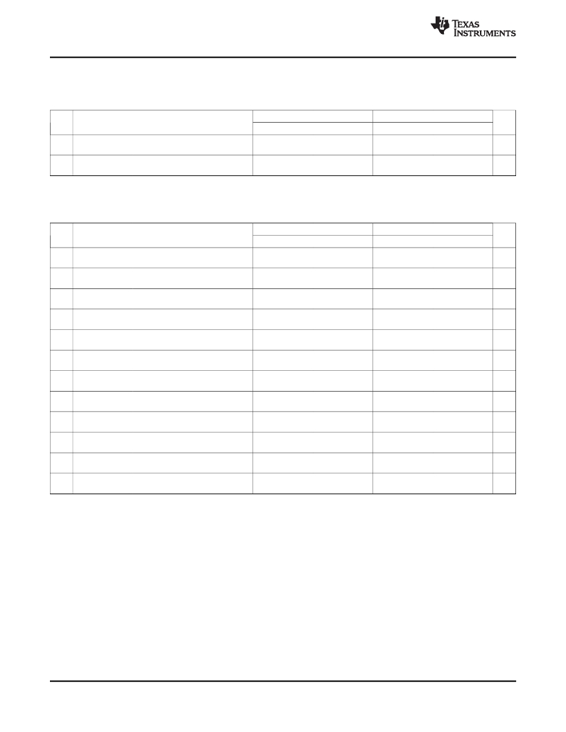
5.15.2 LCDC Electrical Data/Timing
NO.
CV DD = 1.05 V
MIN MAX
MIN
CV DD = 1.3 V
MAX
UNIT
16
17
t su(LCD_D-CLK)
t h(CLK-LCD_D)
Setup time, LCD_D[15:0] valid
before LCD_CLK rising edge
Hold time, LCD_D[15:0] valid after
LCD_CLK rising edge
27
0
42
0
ns
ns
(1)
Over operating free-air temperature range (unless otherwise noted)
Table 5-42. Switching Characteristics Over Recommended Operating Conditions for LCD LIDD Mode (see
NO.
PARAMETER
CV DD = 1.05 V
MIN MAX
MIN
CV DD = 1.3 V
MAX
UNIT
4
5
6
7
8
9
10
11
12
13
14
15
t d(LCD_D_V)
t d(LCD_D_I)
t d(LCD_E_A)
t d(LCD_E_I)
t d(LCD_A_A)
t d(LCD_A_I)
t d(LCD_W_A)
t d(LCD_W_I)
t d(LCD_STRB_A)
t d(LCD_STRB_I)
t d(LCD_D_Z)
t d(Z_LCD_D)
Delay time, LCD_CLK rising edge
to LCD_D[15:0] valid (write)
Delay time, LCD_CLK rising edge
to LCD_D[15:0] invalid (write)
Delay time, LCD_CLK rising edge
to LCD_CSx_Ex low
Delay time, LCD_CLKrising edge
to LCD_CSx_Ex high
Delay time, LCD_CLKrising edge
to LCD_RS low
Delay time, LCD_CLK rising edge
to LCD_RS high
Delay time, LCD_CLK rising edge
to LCD_RW_WRB low
Delay time, LCD_CLK rising edge
to LCD_RW_WRB high
Delay time, LCD_CLK rising edge
to LCD_EN_RDB high
Delay time, LCD_CLK rising edge
to LCD_EN_RDB low
Delay time, LCD_CLK rising edge
to LCD_D[15:0] in 3-state
Delay time, LCD_CLK rising edge
to LCD_D[15:0] valid from 3-state
-6
-6
-6
-6
-6
-6
5
5
5
5
5
5
-6
-6
-6
-6
-6
-6
7
7
7
7
7
7
ns
ns
ns
ns
ns
ns
ns
ns
ns
ns
ns
ns
126
Peripheral Information and Electrical Specifications
Product Folder Links: TMS320C5515
Copyright ? 2010–2013, Texas Instruments Incorporated
发布紧急采购,3分钟左右您将得到回复。
相关PDF资料
TMDXEXP1808L
KIT EXPERIMENTER FOR AM180X
TO263-3EV-VREG
BOARD EVAL TO220-3/TO263-3 VREG
TO263-5EV-VREG
EVAL BOARD VREG TO220-5/TO263-5
TOOLSTICK-EK
KIT TOOL EVAL SYS IN A USB STICK
TPS23757EVM
EVALUATION MODULE FOR TPS23757
TPS62230EVM-370
EVAL MODULE FOR TPS62230-370
TRAVELCUBE
SURGE SUP 1OUT W/RJ11 DIRECTPLUG
TRAVELER100BT
SURGE SUP 2OUT W/RJ11 DIRECTPLUG
相关代理商/技术参数
TMDXEVM5515
制造商:Texas Instruments 功能描述:TMS320C5515 DSP Evaluation Module
TMDXEVM642
制造商:Texas Instruments 功能描述:Tools Development kit For Use
TMDXEVM6424
功能描述:开发板和工具包 - TMS320 C6424 DSP Eval Mod RoHS:否 制造商:Texas Instruments 产品:Experimenter Kits 工具用于评估:F2802x 核心:TMS320 接口类型:UART, USB 工作电源电压:
TMDXEVM6446
制造商:Rochester Electronics LLC 功能描述:DAVINCI EVM BUNDLE W/O EMULATOR - Bulk 制造商:Texas Instruments 功能描述:DAVINCI EVM BUNDLE W/O EMULATOR - Bulk
TMDXEVM6446T
制造商:Texas Instruments 功能描述:DM6446 DIGITAL VIDEO EVALUATION MODULE - Boxed Product (Development Kits)
TMDXEVM6446TS
制造商:Texas Instruments 功能描述:DM6446 DIGITAL VIDEO EVALUATION MODULE - Trays
TMDXEVM6452
功能描述:开发板和工具包 - TMS320 C6452 EVM Evaluation Module RoHS:否 制造商:Texas Instruments 产品:Experimenter Kits 工具用于评估:F2802x 核心:TMS320 接口类型:UART, USB 工作电源电压:
TMDXEVM6455
功能描述:开发板和工具包 - TMS320 C6455 Evaluation Module RoHS:否 制造商:Texas Instruments 产品:Experimenter Kits 工具用于评估:F2802x 核心:TMS320 接口类型:UART, USB 工作电源电压:
